- 您现在的位置:买卖IC网 > Sheet目录2006 > LTC2306CDD#PBF (Linear Technology)IC ADC 12BIT 2CH 500KSPS 10-DFN
LTC2302/LTC2306
4
23026fa
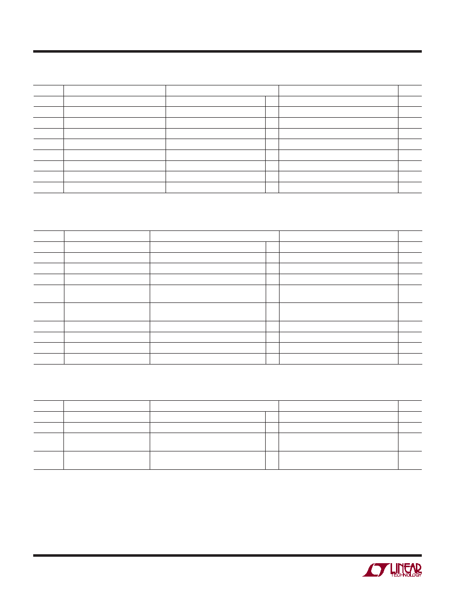
SYMBOL
PARAMETER
CONDITIONS
MIN
TYP
MAX
UNITS
VIH
High Level Input Voltage
VDD = 5.25V
l
2.4
V
VIL
Low Level Input Voltage
VDD = 4.75V
l
0.8
V
IIN
High Level Input Current
VIN = VDD
l
±10
μA
CIN
Digital Input Capacitance
5pF
VOH
High Level Output Voltage
OVDD = 4.75V, IOUT = –10μA
OVDD = 4.75V, IOUT = –200μA
l
4
4.74
V
VOL
Low Level Output Voltage
OVDD = 4.75V, IOUT = 160μA
OVDD = 4.75V, IOUT = 1.6mA
l
0.05
0.4
V
IOZ
Hi-Z Output Leakage
VOUT = 0V to OVDD, CONVST High
l
±10
μA
COZ
Hi-Z Output Capacitance
CONVST High
15
pF
ISOURCE
Output Source Current
VOUT = 0V
–10
mA
ISINK
Output Sink Current
VOUT = OVDD
10
mA
DIGITAL INPUTS AND DIGITAL OUTPUTS The l denotes the specications which apply over the
full operating temperature range, otherwise specications are at TA = 25°C. (Note 4)
SYMBOL
PARAMETER
CONDITIONS
MIN
TYP
MAX
UNITS
VDD
Supply Voltage
l
4.75
5
5.25
V
OVDD
Output Driver Supply Voltage
l
2.7
5.25
V
IDD
Supply Current
Sleep Mode
CL = 25pF
CONVST = 5V, Conversion Done
l
2.8
7
3.5
15
mA
μA
PD
Power Dissipation
Sleep Mode
14
35
mW
μW
POWER REQUIREMENTS The l denotes the specications which apply over the full operating temperature
range, otherwise specications are at TA = 25°C. (Note 4)
SYMBOL
PARAMETER
CONDITIONS
MIN
TYP
MAX
UNITS
SINAD
Signal-to-(Noise + Distortion) Ratio
fIN = 1kHz
l
71
72.8
dB
SNR
Signal-to-Noise Ratio
fIN = 1kHz
l
71
73.2
dB
THD
Total Harmonic Distortion
fIN = 1kHz, First 5 Harmonics
l
–88
–78
dB
SFDR
Spurious Free Dynamic Range
fIN = 1kHz
l
79
89
dB
Channel-to-Channel Isolation
fIN = 1kHz
–109
dB
Full Linear Bandwidth
(Note 11)
700
kHz
–3dB Input Linear Bandwidth
25
MHz
Aperture Delay
13
ns
Transient Response
Full-Scale Step
240
ns
DYNAMIC ACCURACY The l denotes the specications which apply over the full operating temperature range,
otherwise specications are at TA = 25°C. AIN = –1dBFS. (Notes 4, 10)
发布紧急采购,3分钟左右您将得到回复。
相关PDF资料
LTC2351HUH-12#TRPBF
IC ADC 12BIT 1.5MSPS 32-QFN
LTC2351HUH-14#TRPBF
IC ADC 14BIT 1.5MSPS 32-QFN
LTC2355IMSE-14#TRPBF
IC ADC 14BIT 3.5MSPS 10-MSOP
LTC2356IMSE-14#TRPBF
IC ADC 14BIT 3.5MSPS 10-MSOP
LTC2366HTS8#TRPBF
IC ADC 12BIT 3MSPS TSOT23-8
LTC2379HMS-18#PBF
IC ADC 18BIT SPI/SRL 16MSOP
LTC2380HMS-16#TRPBF
IC ADC 16BIT 2MSPS 16-MSOP
LTC2382HMS-16#PBF
IC ADC 16BIT 1CH 500KSPS 16-MSOP
相关代理商/技术参数
LTC2306CDD#TRPBF
功能描述:IC ADC 12-BIT 2CH 500KSPS 10DFN RoHS:是 类别:集成电路 (IC) >> 数据采集 - 模数转换器 系列:- 标准包装:2,500 系列:- 位数:16 采样率(每秒):15 数据接口:MICROWIRE?,串行,SPI? 转换器数目:1 功率耗散(最大):480µW 电压电源:单电源 工作温度:-40°C ~ 85°C 安装类型:表面贴装 封装/外壳:38-WFQFN 裸露焊盘 供应商设备封装:38-QFN(5x7) 包装:带卷 (TR) 输入数目和类型:16 个单端,双极;8 个差分,双极 配用:DC1011A-C-ND - BOARD DELTA SIGMA ADC LTC2494
LTC2306IDD#PBF
功能描述:IC ADC 12BIT 2CH 500KSPS 10-DFN RoHS:是 类别:集成电路 (IC) >> 数据采集 - 模数转换器 系列:- 标准包装:2,500 系列:- 位数:16 采样率(每秒):15 数据接口:MICROWIRE?,串行,SPI? 转换器数目:1 功率耗散(最大):480µW 电压电源:单电源 工作温度:-40°C ~ 85°C 安装类型:表面贴装 封装/外壳:38-WFQFN 裸露焊盘 供应商设备封装:38-QFN(5x7) 包装:带卷 (TR) 输入数目和类型:16 个单端,双极;8 个差分,双极 配用:DC1011A-C-ND - BOARD DELTA SIGMA ADC LTC2494
LTC2306IDD#TRPBF
功能描述:IC ADC 12-BIT 2CH 500KSPS 10DFN RoHS:是 类别:集成电路 (IC) >> 数据采集 - 模数转换器 系列:- 标准包装:2,500 系列:- 位数:16 采样率(每秒):15 数据接口:MICROWIRE?,串行,SPI? 转换器数目:1 功率耗散(最大):480µW 电压电源:单电源 工作温度:-40°C ~ 85°C 安装类型:表面贴装 封装/外壳:38-WFQFN 裸露焊盘 供应商设备封装:38-QFN(5x7) 包装:带卷 (TR) 输入数目和类型:16 个单端,双极;8 个差分,双极 配用:DC1011A-C-ND - BOARD DELTA SIGMA ADC LTC2494
LTC2308CUF#PBF
功能描述:IC ADC 12BIT 8CH 500KSPS 24-QFN RoHS:是 类别:集成电路 (IC) >> 数据采集 - 模数转换器 系列:- 标准包装:1,000 系列:- 位数:16 采样率(每秒):45k 数据接口:串行 转换器数目:2 功率耗散(最大):315mW 电压电源:模拟和数字 工作温度:0°C ~ 70°C 安装类型:表面贴装 封装/外壳:28-SOIC(0.295",7.50mm 宽) 供应商设备封装:28-SOIC W 包装:带卷 (TR) 输入数目和类型:2 个单端,单极
LTC2308CUF#PBF
制造商:Linear Technology 功能描述:A/D Converter (A-D) IC
LTC2308CUF#TRPBF
功能描述:IC ADC 12BIT 500KSPS 24-QFN RoHS:是 类别:集成电路 (IC) >> 数据采集 - 模数转换器 系列:- 标准包装:1,000 系列:- 位数:16 采样率(每秒):45k 数据接口:串行 转换器数目:2 功率耗散(最大):315mW 电压电源:模拟和数字 工作温度:0°C ~ 70°C 安装类型:表面贴装 封装/外壳:28-SOIC(0.295",7.50mm 宽) 供应商设备封装:28-SOIC W 包装:带卷 (TR) 输入数目和类型:2 个单端,单极
LTC2308CUFPBF
制造商:Linear Technology 功能描述:ADC 12-Bit 8-Ch 500Ksps Low Noise QFN24
LTC2308IUF#PBF
功能描述:IC ADC 12BIT 8CH 500KSPS 24-QFN RoHS:是 类别:集成电路 (IC) >> 数据采集 - 模数转换器 系列:- 标准包装:1 系列:microPOWER™ 位数:8 采样率(每秒):1M 数据接口:串行,SPI? 转换器数目:1 功率耗散(最大):- 电压电源:模拟和数字 工作温度:-40°C ~ 125°C 安装类型:表面贴装 封装/外壳:24-VFQFN 裸露焊盘 供应商设备封装:24-VQFN 裸露焊盘(4x4) 包装:Digi-Reel® 输入数目和类型:8 个单端,单极 产品目录页面:892 (CN2011-ZH PDF) 其它名称:296-25851-6